NPTEL Digital System Design Week 8 Assignment Answers 2025
1. In the given Verilog testbench code snippet, a clock signal is defined as follows:
initial
clock = 1’b0
always
#5 clock = ~clock;
initial
#1000 $finish
How many clock cycles will the simulation run before finishing?
Answer :- For Answers Click Here
2. In the circuit, what will be the output at Q3,Q2,Q1,Q0 after one clock cycle, if input applied is 0010 respectively.
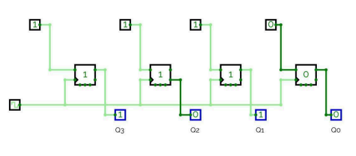
Answer :-
3. In below given logic diagram of 1-bit Register using D flip flop, determine the output at Q for three cycles, as given in the waveform. [Assume no delays, and Q initially = 0]
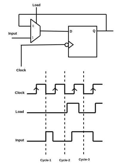
- 011
- 110
- 000
- 101
Answer :-
4. In the below given logic diagram of 4-bit Register using D flip flop, determine the output at out_3, out_2, out_1, out_0 after three cycles, as given in the waveform. [Assume no delays, and Q3Q2Q1Q0 initially = 0]
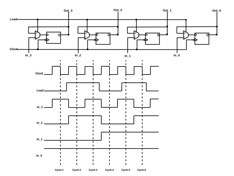
- 1001
- 0010
- 1110
- 1101
Answer :-
5. In the given logic diagram of 4-bit Register using D flip flop, determine the output at out_3, out_2, out_1, out_0 after six cycles, as given in the waveform. [Assume no delays, and Q3Q2Q1Q0 initially = 0] [Logic diagram is same as in Question-4]
- 1001
- 0010
- 1110
- 0111
Answer :-
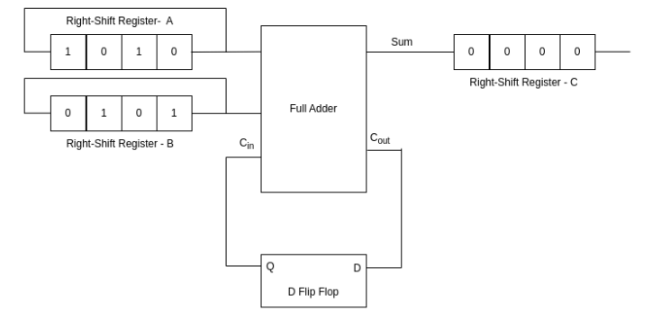
6. what will be the possible values of shift register-A, shift register-B, shift register-C after 3 clock pulses
- 0111, 0010, 1100
- 0111, 0010, 1110
- 0101, 1010, 1110
- 0111, 1010, 1100
Answer :-
7. what will be the possible values of shift register-A, shift register-B, shift register-C and DFF after 4 clock pulses
- 0111, 0010, 1100
- 1010, 0101, 1111
- 0101, 1010, 1110
- 0111, 1010, 1100
Answer :-
8. Evaluate the provided Verilog code for a module named “exp1”:
module exp1 (select, BitPosition);
input [5:1] select;
output [2:0] BitPosition;
reg [2:0] BitPosition;
always @ (select)
  casex (select)
    5'bxxxx1: BitPosition = 1;
    5'bxxx1x: BitPosition = 2;
    5'bxx1xx: BitPosition = 3;
    5'b1xxxx: BitPosition = 5;
  endcase
endmodule
What would be the value of BitPosition if select = 5 (decimal)?
- 1
- 2
- 3
- 5
- undefined
Answer :-
9. With a 200 kHz clock frequency, eight bits can be serially entered into a shift register in _______.
- 40000 ps
- 60000 ps
- 40000 ns
- 60000 ns
Answer :-
Linked Question 10 and 11
In a microprocessor, registers are utilized to store data before presenting them to the Arithmetic Logic Unit (ALU) for computation. In the given scenario, there are two 8-bit Serial-In Parallel-Out (SIPO) registers depicted in the figure given below. The objective is to serially shift two 8-bit data into these registers and then perform addition between them. The CPU operates with a clock frequency of 5 GHz, and the ALU requires 2 clock cycles to perform addition once the data is available at its input.
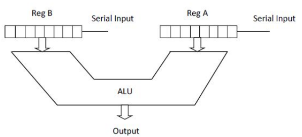
10. Identify the number of clock cycles required to load the data into the registers_______?
Answer :- For Answers Click Here
11. Calculate the time required to load and perform addition of two 8-bit numbers.(The data from both registers is available parallely at the input of ALU).
- 2 ns
- 4 ns
- 4 ms
- 2 ms
Answer :-
12. With a clock frequency of 400 kHz, consider a 32-bit parallel-in serial-out (PISO) register. Calculate the total time required to store (load data in parallel) and access (shift out serially) all 32 bits of data from the register.
- 82.5 microseconds
- 20.5 microseconds
- 50 microseconds
- 30.5 microseconds
Answer :-
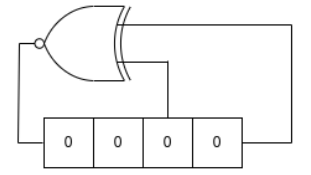
13. what will be output [data_out] after clock pulse 3? [Enter Answer in Hexa]
Answer :-
14. what will be output [data_out] after clock pulse 4? [Enter Answer in Hexa]
Answer :-
15. In a 4-bit right shift register, how many clock pulses are required to change the content of register all 0’s
- 12 clock pulses
- 15 clock pulses
- 8 clock pulses
- 4 clock pulses
- not a possible state
Answer :- For Answers Click Here