NPTEL Digital System Design Week 5 Assignment Answers 2025
1. In an IoT node system, the stop condition is defined by the Boolean expression S=M+E+D′, where:
● M: Manual stop
● E: Error occurred
● D: Data available (D’: No data available)
● S: Stop
Under what condition will the system NOT stop?
- Manual stop button is pressed, and data is available.
- An error occurred, and data is available.
- Manual stop button is not pressed, no error occurred, and data is available.
- Manual stop button is not pressed, an error occurred, and no data is available.
Answer :- For Answers Click Here
2. The circuit in the diagram consists of four 4-to-1 multiplexers in the first stage, which are connected to a single 4-to-1 multiplexer in the second stage. The input lines are labeled I0
to I15, and the select lines are C3C2C1C0.

If the select inputs are C3C2C1C0 = 1011, identify the selected input Ix that will appear as the output Z.
- Z = I8
- Z = I9
- Z = I10
- Z = I11
Answer :-
3. A certain multiplexer can switch one of 64 inputs to its output. How many different inputs does this multiplexer have?
- 64 data inputs and 6 select inputs
- 64 select inputs and 6 data inputs
- 6 data inputs and 6 select inputs
- Such a MUX cannot be implemented
- None of the above
Answer :-
Q.No.4 to Q.No.7 are linked questions.

The memory system in the diagram consists of 16 memory cells, each storing 8 bits of data. If the system is upgraded to support 32 memory cells with the same data width, how many address lines will now be required to access all memory cells?
- 4
- 5
- 6
- 8
Answer :-
5. If memory cell M7 contains the binary data 11110000 and cell M12 contains 01010101, what will be the output at DataOut if:
● The address is set to 1100,
● The DataIn line provides 10101010,
● Write Enable (W) is 0?
- 1110000
- 01010101
- 10101010
- Undefined
Answer :-
6. Consider the following situation:
● DataIn is 10011001,
● Address is set to 0011,
● Write Enable (W) is 1,
After the operation, if the address remains 0011 and W is set to 0, what will be the output at DataOut?
- 00000000
- 10011001
- 1111 1111
- Undefined
Answer :-
7. The memory system stores data in 16 cells, each of 8 bits. If the address bus is expanded to 6 bits with the mux configuration changes to fit this width, and each cell can now store 16 bits, what is the new total memory capacity in bytes?
- 32 bytes
- 64 bytes
- 128 bytes
- 256 bytes
Answer :-
8. A ROM implements the following Boolean functions. What will be the minimum size of the ROM?
F1(A,B,C)=AB+AC′
F2(A,B,C)=A′C+BC
F3(A,B,C)=A′B+ABC′
- 2^3 × 2
- 2^3 × 3
- 2^2 × 3
- 2^3 × 4
- None of the above
Answer :-
9. Consider the circuit in the figure.

Determine the state of P1, P2, and Output if the inputs and control signals are set as follows:
● A = 0, B = 1, C = 1, D = 0
● Control 1 = 1, Control 2 = 1, Control 3 = 0
- P1 = 0, P2 = 1, Output = 1
- P1 = 1, P2 = 0, Output = 0
- P1 = 0, P2 = 1, Output = 0
- P1 = 1, P2 = 0, Output = 1
Answer :- For Answers Click Here
10. How many total addresses are required in a memory of size 8 KBytes if the memory is byte-addressable?
- 2048
- 4096
- 8192
- 1024
Answer :-
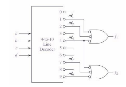
11. Which out of the following function is implemented by the given diagram:

- Z = A’C +A’BC + AB’D’
- Z = A’C +A’BC’ + AB’
- Z = A’C’ +A’BD’ + AB’D’
- Z = A’BC +A’BD + A’B’D’
Answer :-
12.
The decoder given in the figure can be used as a 3-to-8-line decoder. To achieve this:
- Which three lines should be used as inputs?
- What should the remaining input line be set to?
- 1. Lines A, B, C
2. Set the remaining line (D) to 1 - 1. Lines B, C, D
2. Set the remaining line (A) to 0 - 1. Lines A, C, D
2. Set the remaining line (B) to 0 - 1. Lines B, C, D
2. Set the remaining line (C) to 1
Answer :-
13. Which of the following statements about Field Programmable Gate Arrays (FPGAs) is true?
- FPGAs have fixed logic and programmable interconnect.
- FPGAs have programmable logic and fixed interconnect.
- FPGAs have programmable logic and programmable interconnect.
- None of the above.
Answer :- For Answers Click Here